3-Terminal Adjustable Negative Voltage Regulator D
3 year ago
3-Terminal Adjustable Negative Regulator D337
DESCRIPTIONS:
The D337 are adjustable 3-terminal negative voltage regulators capable of supplying in excess of − 1.5A over an output voltage
range of − 1.2 V to − 37V. These regulators are exceptionally easy to apply, requiring only 2 external resistors to set the output voltage and 1 output capacitor for frequency compensation. The circuit
design has been optimized for excellent regulation and low thermal transients.
The D337 serve a wide variety of applications including local on-card regulation, programmable-output voltage regulation or
precision current regulation. The D337 is ideal complements to the D337 adjustable positive regulators.
FEATURES
Output voltage adjustable from − 1. 2 V to − 37 V
1.5A output current guaranteed, − 55°C to + 150°C
Line regulation typically 0.01%/V
Excellent thermal regulation, 0. 002%/W
Excellent rejection of thermal transients
Temperature-independent current limit
Internal thermal overload protection
77 dB ripple rejection
50 ppm/°C temperature coefficient
Load regulation typically 0.3 %
P+ Product Enhancement tested
Output is short circuit protected
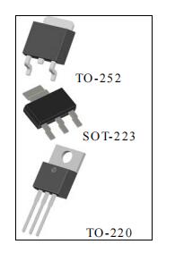
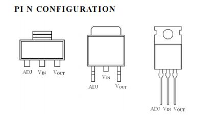
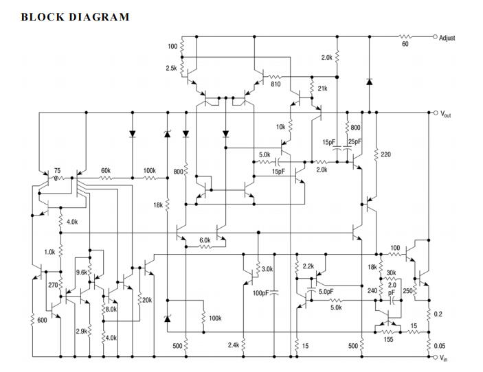
ABSOLUTE MAXIMUM RATINGS *1
Characteristic
Va lue
Unit
Power dissipation
Internally l imited
Input-output voltage differential
40
V
Operating junction temperature range
0 ~ +125
°C
Storage temperature
-65 ~ +150
°C
Lead temperature (soldering, 10 sec.)
300
°C
Plastic package (soldering, 4 sec.)
260
°C
ESD rating
2k
Volts
ELECTRICAL CHARACTERISTICS *1
Characteristics
Test conditions
Min
Typ
Max
Unit
Line regulation
Tj=25°C,3V≤∣VIN-VOUT∣≤40V
*2 IL=10mA
0.01
0.04
%/V
Load regulation
Tj=25°C, 10mA≤IOUT≤IMAX
0.3
1.0
%
Thermal regulation
Tj=25°C, 10ms pulse
0.003
0.04
%/W
Adjustment pin current
65
100
µ A
Adjustment pin current charge
10mA≤IL≤IMAX,TA=25°C
3V≤∣VIN-VOUT∣≤40V
2
5
µ A
Reference voltage
Tj=25°C *3
3V≤∣VIN-VOUT∣≤40V *3
10mA≤IOUT≤IMAX, P≤PMAX
-1.213
-1.200
-1.250
-1.250
-1.287
-1.300
V
Line regulation
3V≤∣VIN-VOUT∣≤40V *2
0.02
0.07
%/V
Load regulation
10mA≤IOUT≤IMAX *2
0.3
1.5
%
Temperature stability
TMIN≤Tj≤TMAX
0.6
%
Minimum load current
∣VIN-VOUT∣≤40V
∣VIN-VOUT∣≤10V
2.5
1.5
10
6
mA
Current limit
∣VIN-VOUT∣≤15V
∣VIN-VOUT∣=40V, Tj=25°C
1.5
0.15
2.2
0.4
3.7
A
RMS output noise,% of VOU T
Tj=25°C, 10Hz≤f≤10kHz
0.003
%
Ripple rejection ratio
VOU T =-10 V, f=120Hz CADJ =10 µ F
66
60
77
dB
Long-term stability
Tj=125°C, 1000 Hours
0.3
1
%
Thermal resistance, junction to case
SOT223 TO-220
TO-252
2.3
12
4
3
15
° C/W
Thermal resistance, junction to ambient (no heat sink)
SOT223 TO-220
TO-252
35
140
50
° C/W
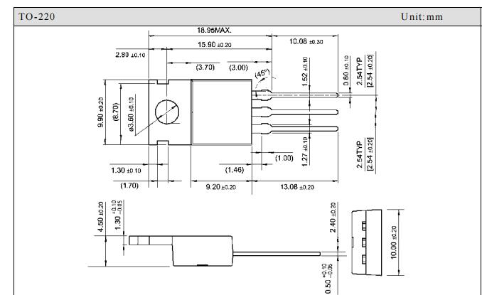
3-Terminal Adjustable Negative Regulator D337
DESCRIPTIONS:
The D337 are adjustable 3-terminal negative voltage regulators capable of supplying in excess of − 1.5A over an output voltage
range of − 1.2 V to − 37V. These regulators are exceptionally easy to apply, requiring only 2 external resistors to set the output voltage and 1 output capacitor for frequency compensation. The circuit
design has been optimized for excellent regulation and low thermal transients.
The D337 serve a wide variety of applications including local on-card regulation, programmable-output voltage regulation or
precision current regulation. The D337 is ideal complements to the D337 adjustable positive regulators.
FEATURES
Output voltage adjustable from − 1. 2 V to − 37 V
1.5A output current guaranteed, − 55°C to + 150°C
Line regulation typically 0.01%/V
Excellent thermal regulation, 0. 002%/W
Excellent rejection of thermal transients
Temperature-independent current limit
Internal thermal overload protection
77 dB ripple rejection
50 ppm/°C temperature coefficient
Load regulation typically 0.3 %
P+ Product Enhancement tested
Output is short circuit protected


ABSOLUTE MAXIMUM RATINGS *1
Characteristic
Va lue
Unit
Power dissipation
Internally l imited
Input-output voltage differential
40
V
Operating junction temperature range
0 ~ +125
°C
Storage temperature
-65 ~ +150
°C
Lead temperature (soldering, 10 sec.)
300
°C
Plastic package (soldering, 4 sec.)
260
°C
ESD rating
2k
Volts
ELECTRICAL CHARACTERISTICS *1
Characteristics
Test conditions
Min
Typ
Max
Unit
Line regulation
Tj=25°C,3V≤∣VIN-VOUT∣≤40V
*2 IL=10mA
0.01
0.04
%/V
Load regulation
Tj=25°C, 10mA≤IOUT≤IMAX
0.3
1.0
%
Thermal regulation
Tj=25°C, 10ms pulse
0.003
0.04
%/W
Adjustment pin current
65
100
µ A
Adjustment pin current charge
10mA≤IL≤IMAX,TA=25°C
3V≤∣VIN-VOUT∣≤40V
2
5
µ A
Reference voltage
Tj=25°C *3
3V≤∣VIN-VOUT∣≤40V *3
10mA≤IOUT≤IMAX, P≤PMAX
-1.213
-1.200
-1.250
-1.250
-1.287
-1.300
V
Line regulation
3V≤∣VIN-VOUT∣≤40V *2
0.02
0.07
%/V
Load regulation
10mA≤IOUT≤IMAX *2
0.3
1.5
%
Temperature stability
TMIN≤Tj≤TMAX
0.6
%
Minimum load current
∣VIN-VOUT∣≤40V
∣VIN-VOUT∣≤10V
2.5
1.5
10
6
mA
Current limit
∣VIN-VOUT∣≤15V
∣VIN-VOUT∣=40V, Tj=25°C
1.5
0.15
2.2
0.4
3.7
A
RMS output noise,% of VOU T
Tj=25°C, 10Hz≤f≤10kHz
0.003
%
Ripple rejection ratio
VOU T =-10 V, f=120Hz CADJ =10 µ F
66
60
77
dB
Long-term stability
Tj=125°C, 1000 Hours
0.3
1
%
Thermal resistance, junction to case
SOT223 TO-220
TO-252
2.3
12
4
3
15
° C/W
Thermal resistance, junction to ambient (no heat sink)
SOT223 TO-220
TO-252
35
140
50
° C/W


ABSOLUTE MAXIMUM RATINGS *1
|
Characteristic |
Va lue |
Unit |
|
Power dissipation |
Internally l imited |
|
|
Input-output voltage differential |
40 |
V |
|
Operating junction temperature range |
0 ~ +125 |
°C |
|
Storage temperature |
-65 ~ +150 |
°C |
|
Lead temperature (soldering, 10 sec.) |
300 |
°C |
|
Plastic package (soldering, 4 sec.) |
260 |
°C |
|
ESD rating |
2k |
Volts |
ELECTRICAL CHARACTERISTICS *1
|
Characteristics |
Test conditions |
Min |
Typ |
Max |
Unit |
|
Line regulation |
Tj=25°C,3V≤∣VIN-VOUT∣≤40V *2 IL=10mA |
|
0.01 |
0.04 |
%/V |
|
Load regulation |
Tj=25°C, 10mA≤IOUT≤IMAX |
|
0.3 |
1.0 |
% |
|
Thermal regulation |
Tj=25°C, 10ms pulse |
|
0.003 |
0.04 |
%/W |
|
Adjustment pin current |
|
|
65 |
100 |
µ A |
|
Adjustment pin current charge |
10mA≤IL≤IMAX,TA=25°C 3V≤∣VIN-VOUT∣≤40V |
|
2 |
5 |
µ A |
|
Reference voltage |
Tj=25°C *3 3V≤∣VIN-VOUT∣≤40V *3 10mA≤IOUT≤IMAX, P≤PMAX |
-1.213 -1.200 |
-1.250 -1.250 |
-1.287 -1.300 |
V |
|
Line regulation |
3V≤∣VIN-VOUT∣≤40V *2 |
|
0.02 |
0.07 |
%/V |
|
Load regulation |
10mA≤IOUT≤IMAX *2 |
|
0.3 |
1.5 |
% |
|
Temperature stability |
TMIN≤Tj≤TMAX |
|
0.6 |
|
% |
|
Minimum load current |
∣VIN-VOUT∣≤40V ∣VIN-VOUT∣≤10V |
|
2.5 1.5 |
10 6 |
mA |
|
Current limit |
∣VIN-VOUT∣≤15V ∣VIN-VOUT∣=40V, Tj=25°C |
1.5 0.15 |
2.2 0.4 |
3.7 |
A |
|
RMS output noise,% of VOU T |
Tj=25°C, 10Hz≤f≤10kHz |
|
0.003 |
|
% |
|
Ripple rejection ratio |
VOU T =-10 V, f=120Hz CADJ =10 µ F |
66 |
60 77 |
|
dB |
|
Long-term stability |
Tj=125°C, 1000 Hours |
|
0.3 |
1 |
% |
|
Thermal resistance, junction to case |
SOT223 TO-220 TO-252 |
|
2.3 12 4 |
3 15 |
° C/W |
|
Thermal resistance, junction to ambient (no heat sink) |
SOT223 TO-220 TO-252 |
|
35 140 50 |
|
° C/W |

Similar Video Recommendation
You May Also Like
If you are interested in the product, contact Bossgoovideo.com for more information
- *To:
- YANGZHOU POSITIONING TECH CO., LTD.
- *Message:
-
Submit
Main Product:
Semiconductor Triac ,
Semiconductor Thyristor,
Semiconductor Module,
Power Diode,
Silicon Transistor,
Bridge Rectifier
You May Also Like


