YZPST-M2G0080120D N-Channel Power MOSFET
3 year agoM2G0080120D
1200V N-Channel Silicon Carbide Power MOSFET SiC MOSFET
Features
• Optimized package with separate driver source pin
• High blocking voltage with low on-resistance
• High-speed switching with low capacitances
• Fast intrinsic diode with low reverse recovery (Qrr)
• Easy to parallel
• RoHS compliant
Benefits
• Higher System Efficiency
• Reduce cooling requirements
• Increased power density
• Enabling higher frequency
• Minimize gate ringing
• Reduction of system complexity and cost
Applications
• Switch Mode Power Supplies
• DC/DC converters
• Solar Inverters
• Battery Chargers
• Motor Drives

Maximum Ratings (Tc = 25 °C unless otherwise specified )
| Symbol | Parameter | Value | Unit | Test Conditions | Note |
| f^DSmax | Drain-Source Breakdown Voltage | 1200 | V | 海=0 V, /d=100 卩A | |
| Id | Continuous Drain Current | 42 | A | 4s=20 V Tc=25 °C | Fig. 18 |
| Pd | Power Dissipation | 208 | W | *=25 °C | Fig. 19 |
| FgS,op | Recommend Gate Source Voltage | -0.25 | V | ||
| J^Smax | Maximum Gate Source Voltage | -0.4 | V | AC (f>lHz) | Note 1 |
| Tj, Tstg | Operating Junction and Storage Temperature Range | -55 to | °C | ||
| 175 | |||||
| 7l | Soldering Temperature | 260 | °C |
Electrical Characteristics
| Symbol | Parameter | Min. | Typ. | Max. | Unit | Test Conditions | Note |
| Static | |||||||
| BVds | Drain-Source Breakdown Voltage | 1200 | - | - | V | 4s=0 V, Zd=100 卩A | |
| A)ss | Zero Gate Voltage Drain Current | — | 11 | 100 | 丹s=1200 V Pgs=0 V | ||
| Igss | Gate-Source Leakage | — | 10 | 250 | nA | 4s=20 V | |
| FGS(th) | Gate-Source Threshold Voltage | 2 | — | 4 | V | Id=5 mA, | Fig. 11 |
| &DS(on) | Drain-Source On-Resistance | — | 78 | 100 | mQ | 国=20 V, Zd=20 A | Fig. 6 |
| Dynamic | |||||||
| Ciss | Input Capacitance | — | 1128 | PF | 4s=0 V,比s=1000 V | Fig. 17 | |
| C^oss | Output Capacitance | — | 86 | f^l.OMHz,瓜=25 mV | |||
| Crss | Reverse Transfer Capacitance | — | 5 | ||||
| Eoss | Coss Stored Energy | - | 44 | 卩J | Fig. 16 | ||
| Qs | Total Gate Charge | — | 52 | nC | moo V | Fig. 12 | |
| figs | Gate-Source Charge | - | 17 | 血=20 A | |||
| Qgd | Gate-Drain Charge | - | 15 | Fgs=-5/+20 V | |||
| td(cn) | Turn-on Delay Time | — | 41 | ns | 丹 s=800 V | ||
| tr | Turn-on Rise Time | - | 21 | Fgs=-5/+20 V | |||
| Turn-off Delay Time | — | 48 | Id=20A | ||||
| tf | Turn-off Fall Time | — | 16 | Ro(ext)=2.5 Q | |||
| RG(int) | Internal Gate Resistance | - | 4 | n | E.O MHz, Vac=25 mV | ||
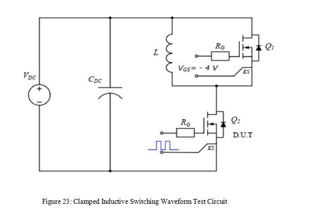
Test Circuit Schematic

SiC MOSFET
Similar Video Recommendation
You May Also Like
If you are interested in the product, contact Bossgoovideo.com for more information
- *To:
- YANGZHOU POSITIONING TECH CO., LTD.
- *Message:
-
Submit
Main Product:
Semiconductor Triac,
Semiconductor Thyristor,
Semiconductor Module,
Power Diode,
Silicon Transistor ,
Bridge Rectifier
You May Also Like


